Avatar

FSPCBA FSPCBA

0 Followers   0 Following

Follow

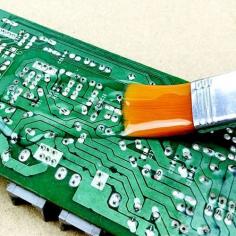
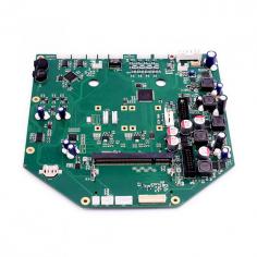
FS Technology is a company dedicated to pcb manufacturing and pcb assembly, located in Shenzhen, China. Here, we will introduce some information about our company and our view on the circuit board industry. If you are interested in us, welcome to our website.

The development of medical equipment PCB in Japan Due to the impact of the new crown epidemic, the Japanese government is increasing investment in medical semiconductor-related industries, such as PCB, circuit board components, assembly industries, etc., which has strengthened the development capabilities of medical PCBA. This reform is to reduce the dependence on importing medical electronics from developed countries such as Europe and the United States. In response to this call, the central government released the "New Medical PCBA Policy" in May 2022. The policy accelerates the growth of Japan's PCBA industry through research and innovation of advanced manufacturing and assembly technologies to promote high value-added industrial chains. Through this policy, Japan may become the second largest PCBA industrial country after China. https://www.fs-pcba.com/medical-pcb/ According to the "New Medical PCBA Policy", the Japanese government believes that the PCBA industry will achieve an economic value target of 1 trillion in 2026 with the support of the government. According to reports, with the outbreak of the new crown epidemic, the global demand for the medical industry is expanding. So far, the annual output value of Japan's medical PCB has reached 2 billion US dollars. Medical PCB is a more difficult circuit board to manufacture. With the "New Medical PCBA Policy", the overall PCB manufacturing industry in Japan will be greatly improved. Goals of the medical PCBA industry in 2023 Generate $2 billion in electronics manufacturing and exports across the PCBA value chain, creating foreign exchange opportunities through import substitution and export promotion; The medical electronics industry will add 50,000 jobs in 2028; Promoting financial and non-financial industries through the development of medical PCB manufacturing; Establish cooperation with more PCBA manufacturers to form an economy that can quickly serve and medical electronics; Establish human resources foundation for the medical industry; https://www.fs-pcba.com/ Encourage R&D and innovation activities in the medical electronics industry. More Qualified Medical Electronics Manufacturers In order to produce more qualified medical electronic products, the Japanese government has set up more "new units" so that qualified manufacturers can be screened out, and these manufacturers must meet the following conditions: Manufacture of electronic products such as telecommunication systems/mobile phones/IT systems and hardware/home appliances/medical electronics/aviation electronics/industrial electronics/defense and strategic electronics/automotive electronics/information and broadcasting equipment. Intermediate parts such as printed circuit boards/semiconductors/semiconductor parts/integrated circuits (ICs)/components/parts. Electronic Contract Manufacturing Services (EMS). Other electronics industries/products covered by the National Electronics Policy (NPE) or other policies issued by the Japanese government from time to time. Funding Support for Medical Electronics A. Financial support for venue, equipment, technology, etc. The manufacturing of medical electronics needs to be designed into many aspects, such as circuit design, PCB manufacturing, assembly, testing, packaging and processing. For high-precision medical PCBs, more professional equipment and technology are required to prevent problems such as EMI. The government provides PCBA manufacturers with a lot of advanced equipment such as, 10-drive wave soldering, automatic SMT machines, laser scanners, etc. Associated utilities include critical equipment needed in the work area, such as private power generation, wastewater treatment facilities, clean rooms, air curtains, air conditioning and air quality control systems, compressed air, water and power supply, and control systems. Related utilities also include manufacturing-related IT and International Industrial Manufacturing Technology (ITES) infrastructure such as servers, software, and enterprise resource planning (ERP) solutions. B. Construction expenditure Expenditures incurred by qualified units for the construction of factories necessary for the production of goods or the provision of labor services. However, it does not include the cost of purchasing land and buildings. https://www.fs-pcba.com/manufacturing-pcb/

Thumb

0 repins 0 comments

Basic knowledge of PCB boards you need This article is mainly aimed at newbies in the PCBA industry or friends who want to enter the PBCA manufacturing industry. In this article, FS Technology will introduce some simple PCB knowledge to you, hoping to help you understand this content. Classification of PCB boards single panel FS Technology believes that this is the simplest and most basic circuit board that all turnkey PCB assembly companies can complete. Its parts are concentrated on one side of the circuit board, and the wires are concentrated on the other side. Because the wires only appear on one side, this kind of PCB is called a single-sided (Single-sided). When the circuit board industry was not very developed, the craftsmanship and production capacity were poor. This board had many strict restrictions on the design circuit (because there is only one side, the wiring cannot cross and must go around a separate path), so this board is used. Double panel For turnkey PCB companies, this type of circuit board is no problem. This board has traces on both sides, but to use two-sided traces, there must be a proper circuit connection between the two sides. Such "bridges" between circuits are called vias. Vias are small holes in a PCB, filled or painted with metal, that can be connected to wires on both sides. Because the area of ​​the double-sided board is twice as large as that of the single-sided board, the double-sided board solves the difficulty of the staggered wiring of the single-sided board (which can lead to vias on the other side), and is more suitable for use in more complex circuits than the single-sided board. https://www.fs-pcba.com/ Multilayer board In order to increase the wiring area, single-sided or double-sided wiring boards are often used for multi-layer boards. A printed circuit board with one double-sided inner layer, two single-sided outer layers, or two double-sided inner layers and two single-sided outer layers, alternated by a positioning system and insulating bonding materials and conductive patterns. Printed circuit boards interconnected according to design requirements become four-layer and six-layer printed circuit boards, also known as multi-layer printed circuit boards. This type of circuit board is extremely challenging for PCB manufacturers, and it requires strong PCB manufacturing capabilities to manufacture circuit boards with more layers. The number of layers on the board does not mean that there are several independent wiring layers. In special cases, an empty layer is added to control the thickness of the board. Usually, the number of layers is an even number, including the outermost two layers. Most motherboards are 4 to 8-layer structures, but technically, almost 100-layer PCB boards are possible. Most large supercomputers use fairly multilayered motherboards, but since such computers can be replaced by clusters of many ordinary computers, ultra-multilayered boards are gradually being phased out. Because the number of layers in the PCB is closely combined, it is generally not easy to see the actual number, but it can still be seen if you look closely at the motherboard. Abbreviations on PCBs https://www.fs-pcba.com/manufacturing-pcb/ It is a short of the ground end of the wire. Represents the ground or 0 wire. This ground is not a real ground, but an assumed ground for the application. For the power supply, it is the negative terminal of the power supply. GND (Ground) It is represented as ground or 0 on the circuit diagram and on the circuit board. GND represents the common terminal, it can also be said to be the ground, but this ground is not the real ground. It is the ground assumed by the application, and for the power supply, it is the negative terminal of the power supply. It is different from the earth. Sometimes it needs to be grounded, sometimes it doesn't, depending on the situation. A ground wire is a wire in an electrical system or electronic device that connects to the earth, enclosure or reference potential zero. In general electrical appliances, the ground wire is connected to the casing to prevent electric shock accidents caused by the destruction of the insulation in the casing. The ground wire is the abbreviation of the grounding device, and the ground wire is divided into working grounding and safety grounding. The protective grounding wire that people use to prevent electric shock accidents when using electronic equipment such as household appliances and offices is a safety grounding wire. More PCB knowledge can be found in the FS Technology PCBA blog. FS Technology PCBA blog https://www.fs-pcba.com/pcba-test/ The word "ANT" on the board is the antenna element. An antenna is a transformer that transforms guided waves propagating on a transmission line into electromagnetic waves propagating in an unbounded medium (usually free space) and vice versa. The English in the circuit diagram is the abbreviation of abreviation, sometimes used in combination, ant is the abbreviation of anter, meaning "antenna", antsw is the combination of ant (antenna) and sw (switch), which means antenna switch. rt on the circuit board Rt is a variable resistor, which generally refers to a thermistor or other variable resistors. Its function is to change its own resistance value according to the surrounding temperature, thereby adjusting the resistance of the entire circuit. Other board related terms VDD: supply voltage (unipolar devices; supply voltage (4000 series digital circuits); drain voltage (FET). VCC: Supply Voltage (Bipolar Devices); Supply Voltage (74 Series Digital Circuits). FS Tech pcb component procurement VSS: Ground or Negative Supply. VEE: Negative voltage supply; source (S) of the FET. [h] VPP: Program/Erase Voltage. If your business needs to purchase components, FS Technology can help you. FS Technology has the best pcb component procurement capabilities in China. https://www.fs-pcba.com/smt-pcb-meaning/

Thumb

0 repins 0 comments

Thumb

0 repins 0 comments

Circuit Board Introduction-FS Technology Circuit board is a kind of electronic circuit, which is very common in our life. There are such items in computers, mobile phones and refrigerators. Printed circuit board is also called pcb board aluminum substrate, high frequency board, ultra-thin circuit board, ultra-thin circuit board, Printed (copper etching technology) circuit boards, etc., are the supports for electronic components and the provider of circuit connections for electronic components. The most common printed circuit boards use the method of printing etching resists to produce circuit patterns and circuits, so they are called printed circuit boards or printed circuit boards. Because people want smaller products, mobile phones are getting smaller and smaller, computers are getting smaller and smaller, and the circuit boards of FS Technology have become more and more refined. With the advent of the 21st century, production technology has become more and more developed. The vast majority of PCBs now use etch resists (lamination or coating), and after exposure and development, PCBs are made by etching. The working principle of FS technology pcb PCB is manufactured by many processes, mainly including the following processes, pads, electrical boundaries, mounting holes, vias, components, connectors, wires, filling, etc. If the pcb is distinguished according to the number of layers, it can be divided into the following common types: pcb single-layer board (Single Layer PCB), pcb double-layer board (Double Layer PCB) and pcb multi-layer board (Multi Layer PCB) three types . The main processes of these pcbs have the following functions, each of which is essential: There are metal vias and non-metal vias, where metal vias are used to connect component pins between layers - vias for fixing pcb-mounting holes Components used for connection between pcbs. -connector Used to determine the size of FS Technology's pcb, all components on the pcb must not exceed this boundary - electrical boundary fspcba The surface copper foil conductive layer is separated by the insulating material of the board base, so that the current flows in various components along the pre-designed route to complete functions such as work, amplification, attenuation, modulation, demodulation, coding, etc. - the working principle of pcb https://www.fs-pcba.com/ Metal Hole-Pad for Soldering Component Pins Electrical network copper film-conductor for connecting component pins Copper plating for ground network can effectively reduce impedance-filling FS technology pcb production method Although there are many methods of processing and making PCBs, the traditional rapid board making methods can be mainly divided into two categories: physical methods and chemical methods: ① Physical method: By using many utensils and power tools, the copper that is not needed on the circuit board is manually engraved. This method is not very good, time-consuming and labor-intensive, and has low accuracy. Of course, it is applicable if your circuit board design is relatively simple, but not for complex circuit boards. Features: It is labor-intensive and time-consuming, the precision is not easy to control and there is irreversibility, and the operation requirements are very high. With the development of science and technology, fewer and fewer people use this method, and people are more inclined to use the chemical method. ② Using chemical methods: This method is currently the most used method by FS Technology. People etch away unnecessary copper in a corrosive solution by covering a protective layer on a blank copper clad laminate. Of course, technology has made us more and more advanced. We have developed many ways to achieve the protective layer, the most traditional way of hand painting method, the method of pasting customized self-adhesive, the method of film sensitization, and the method developed in 2010. Thermal transfer printing PCB board method. Features: The process is relatively complex, but the precision is controllable. It is the most widely used rapid plate-making method at present, but there are still many problems. ③ Hand painting: Manually draw the shape of the circuit on the blank copper clad laminate with a soft pen or a hard pen. After drying, it can be put into the solution for direct corrosion. ④ Paste the sticker: There are all kinds of stickers in the world that are made into strips and discs. Different stickers are combined on the blank circuit board as needed, and they can be corroded after they are glued. ⑤ Film sensitivity: printed circuit board The PCB circuit board diagram is printed on the film by a laser printer, and the blank CCL is pre-coated with a layer of photosensitive material (coated CCL is sold in the market), and it can be exposed, developed, fixed and cleaned in a darkroom environment. Corrosion in solution. ⑥ Thermal transfer: The circuit is directly printed on the blank circuit board by the FS technology thermal transfer printer, and then put into the corrosive solution to corrode. To sum up: the previously used physical plate-making method is labor-intensive, time-consuming and low in precision, while the chemical rapid plate-making method has controllable precision, but the process is complex and not environmentally friendly. Regardless of whether it is a physical method or a chemical method, both of them require high operating skills, so neither can be regarded as a good method that can help engineers achieve "fast" board making.

Thumb

0 repins 0 comments